Silicon etching / regeneration
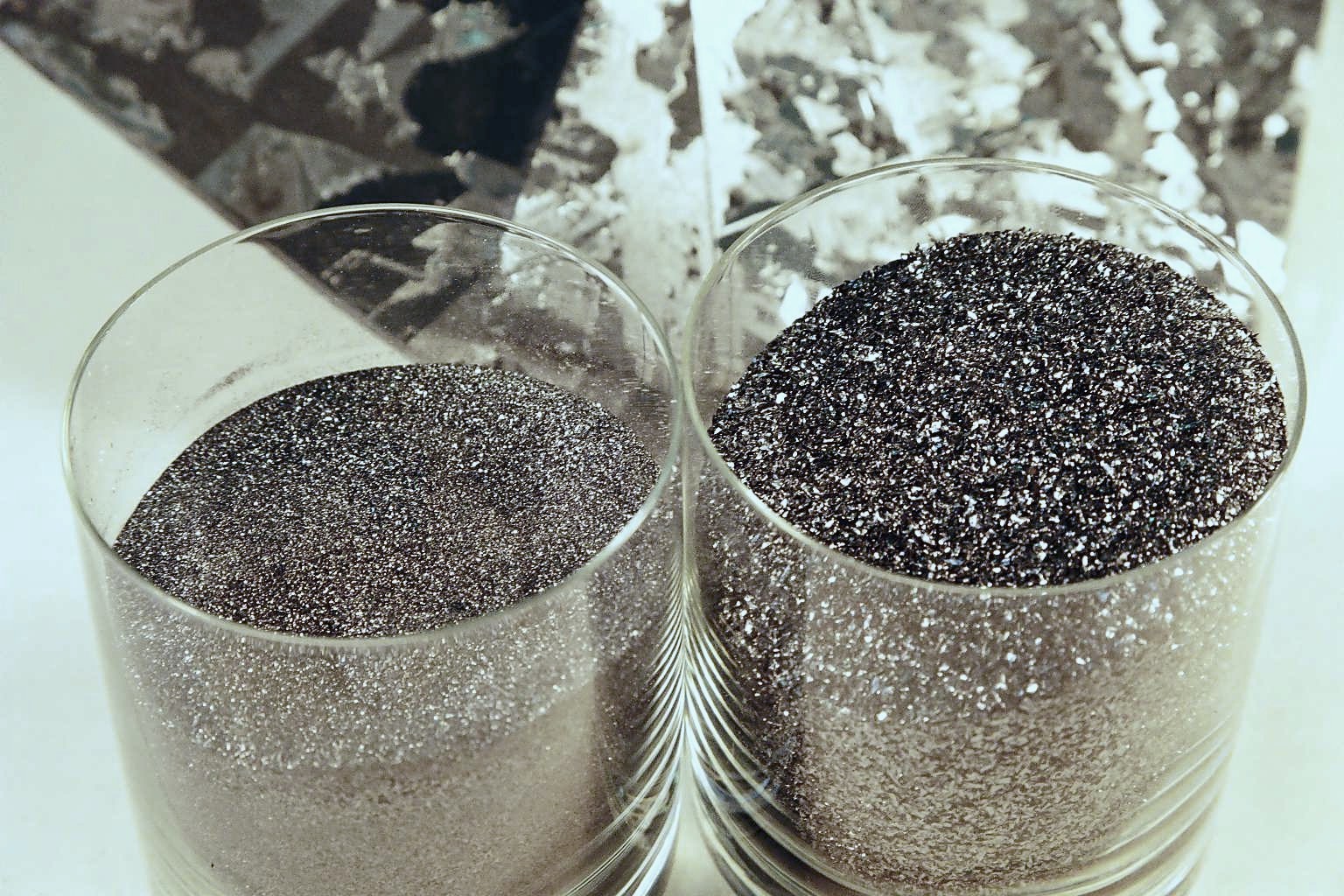
The main reason for silicon etching is to remove and clean the surface of metal and non-metallic impurities as oxides and other chemical compounds. It is mainly achieved by sequence of alternating acidobasic steps which the silicon is going through. This ensures surface pollution removing and flushing released heterogeneous particles out. Those were incorporated by the secondary conversion process (melting, slicing, crushing). An acquirement of pure silicon material which is suitable for following fabrication as a secondary source for photovoltaic applications is then resulted.
Layer properties
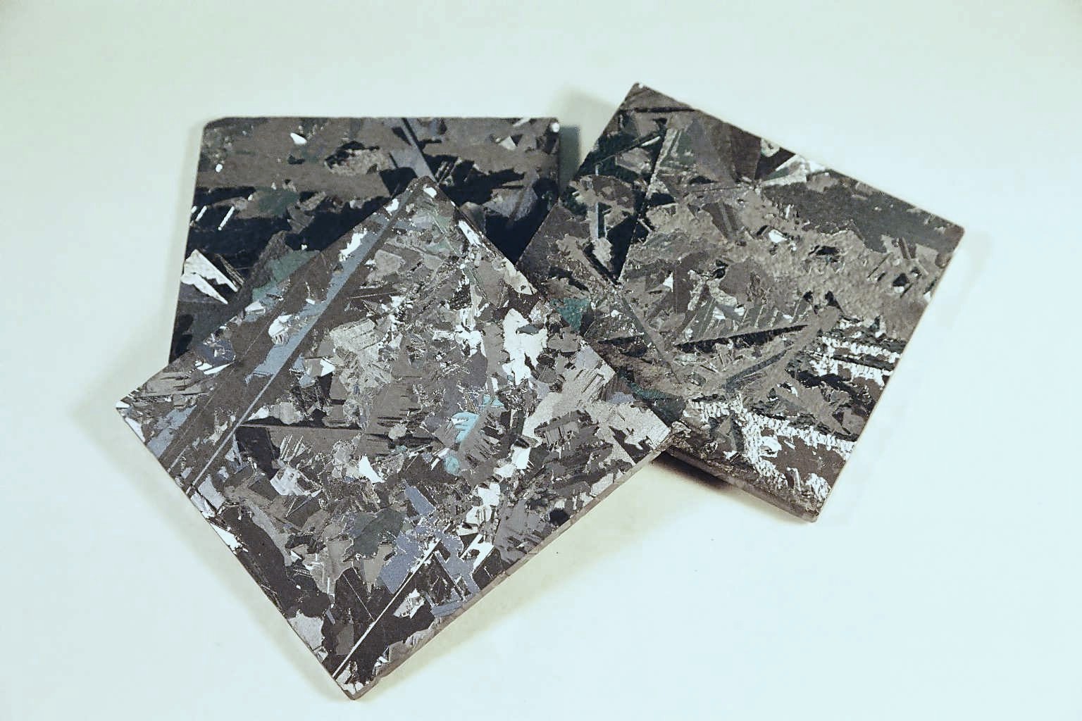
- Bright appearance - free of heterogeneous impurities and chemical substances (oxides, nitrides....)
Deposition - dimension
- In dependence on material constitution and kind of contamination (small-sized bulk material × junk material) 1 μm - hundreds μm
Way of processing
- Free immersion - in baskets and special cartridges
Basic material - substrate:
- Silicon suitable for photovoltaics
Application field:
- Secondary source for photovoltaic cells production